Datasheet Texas Instruments LM3100 — Ficha de datos
| Fabricante | Texas Instruments |
| Serie | LM3100 |
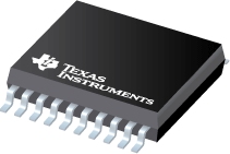
SIMPLE SWITCHER® Regulador de voltaje reductor síncrono de 1MHz y 1.5A
Hojas de datos
LM3100 SIMPLE SWITCHER® Synchronous 1MHz 1.5A Step-Down Voltage Regulator datasheet
PDF, 2.7 Mb, Revisión: G, Archivo publicado: abr 3, 2013
Extracto del documento
Precios
Estado
| LM3100MH | LM3100MH/NOPB | LM3100MHX | LM3100MHX/NOPB | |
|---|---|---|---|---|
| Estado del ciclo de vida | NRND (No recomendado para nuevos diseños) | Activo (Recomendado para nuevos diseños) | NRND (No recomendado para nuevos diseños) | Activo (Recomendado para nuevos diseños) |
| Disponibilidad de muestra del fabricante | No | Sí | No | No |
Embalaje
| LM3100MH | LM3100MH/NOPB | LM3100MHX | LM3100MHX/NOPB | |
|---|---|---|---|---|
| N | 1 | 2 | 3 | 4 |
| Pin | 20 | 20 | 20 | 20 |
| Package Type | PWP | PWP | PWP | PWP |
| Industry STD Term | HTSSOP | HTSSOP | HTSSOP | HTSSOP |
| JEDEC Code | R-PDSO-G | R-PDSO-G | R-PDSO-G | R-PDSO-G |
| Package QTY | 73 | 73 | 2500 | 2500 |
| Carrier | TUBE | TUBE | LARGE T&R | LARGE T&R |
| Device Marking | MH | MH | MH | LM3100 |
| Width (mm) | 4.4 | 4.4 | 4.4 | 4.4 |
| Length (mm) | 6.5 | 6.5 | 6.5 | 6.5 |
| Thickness (mm) | 1 | 1 | 1 | 1 |
| Pitch (mm) | .65 | .65 | .65 | .65 |
| Max Height (mm) | 1.2 | 1.2 | 1.2 | 1.2 |
| Mechanical Data | Descargar | Descargar | Descargar | Descargar |
Paramétricos
| Parameters / Models | LM3100MH | LM3100MH/NOPB | LM3100MHX | LM3100MHX/NOPB |
|---|---|---|---|---|
| Approx. Price (US$) | 1.85 | 1ku | |||
| Control Mode | COT with emulated ripple | COT with emulated ripple | COT with emulated ripple | COT with emulated ripple |
| Duty Cycle(Max), % | 94 | 94 | 94 | |
| Duty Cycle(Max)(%) | 94 | |||
| Iout(Max), A | 1.5 | 1.5 | 1.5 | |
| Iout(Max)(A) | 1.5 | |||
| Iq(Typ), mA | 1 | 1 | 1 | |
| Iq(Typ)(mA) | 1 | |||
| Operating Temperature Range, C | -40 to 125 | -40 to 125 | -40 to 125 | |
| Operating Temperature Range(C) | -40 to 125 | |||
| Package Group | HTSSOP | HTSSOP | HTSSOP | HTSSOP |
| Rating | Catalog | Catalog | Catalog | Catalog |
| Regulated Outputs | 1 | 1 | 1 | |
| Regulated Outputs(#) | 1 | |||
| Special Features | Enable,Synchronous Rectification,Tracking | Enable,Synchronous Rectification,Tracking | Enable Synchronous Rectification Tracking | Enable,Synchronous Rectification,Tracking |
| Switching Frequency(Max), kHz | 1000 | 1000 | 1000 | |
| Switching Frequency(Max)(kHz) | 1000 | |||
| Switching Frequency(Min), kHz | 200 | 200 | 200 | |
| Switching Frequency(Min)(kHz) | 200 | |||
| Type | Converter | Converter | Converter | Converter |
| Vin(Max), V | 36 | 36 | 36 | |
| Vin(Max)(V) | 36 | |||
| Vin(Min), V | 4.5 | 4.5 | 4.5 | |
| Vin(Min)(V) | 4.5 | |||
| Vout(Max), V | 7 | 7 | 7 | |
| Vout(Max)(V) | 7 | |||
| Vout(Min), V | 0.8 | 0.8 | 0.8 | |
| Vout(Min)(V) | 0.8 |
Plan ecológico
| LM3100MH | LM3100MH/NOPB | LM3100MHX | LM3100MHX/NOPB | |
|---|---|---|---|---|
| RoHS | See ti.com | Obediente | TBD | Obediente |
| Pb gratis | No |
Notas de aplicación
- AN-643 EMI/RFI Board Design (Rev. B)PDF, 742 Kb, Revisión: B, Archivo publicado: mayo 3, 2004
Application Note 643 EMI/RFI Board Design - Input and Output Capacitor SelectionPDF, 219 Kb, Archivo publicado: sept 19, 2005
- AN-1197 Selecting Inductors for Buck Converters (Rev. B)PDF, 558 Kb, Revisión: B, Archivo publicado: abr 23, 2013
This application report provides design information to help select an off-the-shelf inductor for anycontinuous-mode buck converter application. - AN-2155 Layout Tips for EMI Reduction in DC/ DC Converters (Rev. A)PDF, 3.6 Mb, Revisión: A, Archivo publicado: abr 23, 2013
This application note will explore how the layout of your DC/DC power supply can significantly affect theamount of EMI that it produces. It will discuss several variations of a layout analyze the results andprovide answers to some common EMI questions such whether or not to use a shielded inductor. - AN-1566 Techniques for Thermal Analysis of Switching Power Supply Designs (Rev. A)PDF, 1.4 Mb, Revisión: A, Archivo publicado: abr 23, 2013
This application note provides thermal power analysis techniques for analyzing the power IC. - AN-1889 How to Measure the Loop Transfer Function of Power Supplies (Rev. A)PDF, 2.7 Mb, Revisión: A, Archivo publicado: abr 23, 2013
This application report shows how to measure the critical points of a bode plot with only an audiogenerator (or simple signal generator) and an oscilloscope. The method is explained in an easy to followstep-by-step manner so that a power supply designer can start performing these measurements in a shortamount of time. - Semiconductor and IC Package Thermal Metrics (Rev. C)PDF, 201 Kb, Revisión: C, Archivo publicado: abr 19, 2016
- AN-1149 Layout Guidelines for Switching Power Supplies (Rev. C)PDF, 82 Kb, Revisión: C, Archivo publicado: abr 23, 2013
When designing a high frequency switching regulated power supply layout is very important. Using agood layout can solve many problems associated with these types of supplies. The problems due to a badlayout are often seen at high current levels and are usually more obvious at large input to output voltagedifferentials. Some of the main problems are loss of regulation at high output current - AN-1229 SIMPLE SWITCHER PCB Layout Guidelines (Rev. C)PDF, 374 Kb, Revisión: C, Archivo publicado: abr 23, 2013
This application report provides SIMPLE SWITCHER™ PCB layout guidelines. - AN-2162 Simple Success With Conducted EMI From DC-DC Converters (Rev. C)PDF, 2.5 Mb, Revisión: C, Archivo publicado: abr 24, 2013
Electromagnetic Interference (EMI) is an unwanted effect between two electrical systems as a result ofeither electromagnetic radiation or electromagnetic conduction. EMI is the major adverse effect caused bythe application of switch-mode power supplies (SMPS). In switching power supplies EMI noise isunavoidable due to the switching actions of the semiconductor devices and resulting disconti - Controlling Output Ripple & Achiev ESR Indep Constant On-Time Reg Designs (Rev. A)PDF, 178 Kb, Revisión: A, Archivo publicado: abr 23, 2013
Of all the voltage regulator control strategies ever devised, the hysteretic regulator is probably about thesimplest. This control methodology simply turns a switch on when the output voltage is below a referenceand turns the switch off when the output rises to a slightly higher reference. The output ripple is thereforea direct function of the difference between the upper and lower reference - AN-1520 A Guide to Board Layout for Best Thermal Resistance for Exposed Packages (Rev. B)PDF, 9.2 Mb, Revisión: B, Archivo publicado: abr 23, 2013
This thermal application report provides guidelines for the optimal board layout to achieve the best thermalresistance for exposed packages. The thermal resistance between junction-to-ambient (ОёJA) is highlydependent on the PCB (Printed Circuit Board) design factors. This becomes more critical for packageshaving very low thermal resistance between junction-to-case such as exposed pad TSSOP
Linea modelo
Serie: LM3100 (4)
Clasificación del fabricante
- Semiconductors> Power Management> Non-isolated DC/DC Switching Regulator> Step-Down (Buck)> Buck Converter (Integrated Switch)