Datasheet Texas Instruments SN74LVTH16541 — Ficha de datos
| Fabricante | Texas Instruments |
| Serie | SN74LVTH16541 |
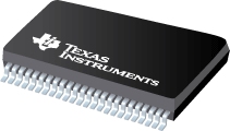
Búferes / controladores ABT de 16 bits y 3.3 V con salidas de 3 estados
Hojas de datos
SN54LVTH16541, SN74LVTH16541 datasheet
PDF, 316 Kb, Revisión: E, Archivo publicado: nov 1, 2006
Extracto del documento
Precios
Estado
| 74LVTH16541DLRG4 | SN74LVTH16541DGGR | SN74LVTH16541DL | SN74LVTH16541DLG4 | SN74LVTH16541DLR | |
|---|---|---|---|---|---|
| Estado del ciclo de vida | Activo (Recomendado para nuevos diseños) | Activo (Recomendado para nuevos diseños) | Activo (Recomendado para nuevos diseños) | Activo (Recomendado para nuevos diseños) | Obsoleto (El fabricante ha interrumpido la producción del dispositivo) |
| Disponibilidad de muestra del fabricante | No | No | No | No | No |
Embalaje
| 74LVTH16541DLRG4 | SN74LVTH16541DGGR | SN74LVTH16541DL | SN74LVTH16541DLG4 | SN74LVTH16541DLR | |
|---|---|---|---|---|---|
| N | 1 | 2 | 3 | 4 | 5 |
| Pin | 48 | 48 | 48 | 48 | 48 |
| Package Type | DL | DGG | DL | DL | DL |
| Industry STD Term | SSOP | TSSOP | SSOP | SSOP | SSOP |
| JEDEC Code | R-PDSO-G | R-PDSO-G | R-PDSO-G | R-PDSO-G | R-PDSO-G |
| Width (mm) | 7.49 | 6.1 | 7.49 | 7.49 | 7.49 |
| Length (mm) | 15.88 | 12.5 | 15.88 | 15.88 | 15.88 |
| Thickness (mm) | 2.59 | 1.15 | 2.59 | 2.59 | 2.59 |
| Pitch (mm) | .635 | .5 | .635 | .635 | .635 |
| Max Height (mm) | 2.79 | 1.2 | 2.79 | 2.79 | 2.79 |
| Mechanical Data | Descargar | Descargar | Descargar | Descargar | Descargar |
| Package QTY | 2000 | 25 | 25 | ||
| Carrier | LARGE T&R | TUBE | TUBE | ||
| Device Marking | LVTH16541 | LVTH16541 | LVTH16541 |
Paramétricos
| Parameters / Models | 74LVTH16541DLRG4 | SN74LVTH16541DGGR | SN74LVTH16541DL | SN74LVTH16541DLG4 | SN74LVTH16541DLR |
|---|---|---|---|---|---|
| Approx. Price (US$) | 0.82 | 1ku | 0.82 | 1ku | |||
| Bits | 16 | 16 | 16 | ||
| Bits(#) | 16 | 16 | |||
| F @ Nom Voltage(Max), Mhz | 160 | 160 | 160 | ||
| F @ Nom Voltage(Max)(Mhz) | 160 | 160 | |||
| ICC @ Nom Voltage(Max), mA | 0.005 | 0.005 | 0.005 | ||
| ICC @ Nom Voltage(Max)(mA) | 0.005 | 0.005 | |||
| Input Type | TTL/CMOS | ||||
| Operating Temperature Range, C | -40 to 85 | -40 to 85 | -40 to 85 | ||
| Operating Temperature Range(C) | -40 to 85 | -40 to 85 | |||
| Output Drive (IOL/IOH)(Max), mA | -32/64 | -32/64 | -32/64 | ||
| Output Drive (IOL/IOH)(Max)(mA) | -32/64 | -32/64 | |||
| Output Type | LVTTL | ||||
| Package Group | SSOP | TSSOP | SSOP | SSOP | SSOP |
| Package Size: mm2:W x L, PKG | 48TSSOP: 101 mm2: 8.1 x 12.5(TSSOP) | 48SSOP: 164 mm2: 10.35 x 15.88(SSOP) | 48SSOP: 164 mm2: 10.35 x 15.88(SSOP) | ||
| Package Size: mm2:W x L (PKG) | 48TSSOP: 101 mm2: 8.1 x 12.5(TSSOP) | 48TSSOP: 101 mm2: 8.1 x 12.5(TSSOP) | |||
| Rating | Catalog | Catalog | Catalog | Catalog | Catalog |
| Schmitt Trigger | No | No | No | No | No |
| Technology Family | LVT | LVT | LVT | LVT | LVT |
| VCC(Max), V | 3.6 | 3.6 | 3.6 | ||
| VCC(Max)(V) | 3.6 | 3.6 | |||
| VCC(Min), V | 2.7 | 2.7 | 2.7 | ||
| VCC(Min)(V) | 2.7 | 2.7 | |||
| Voltage(Nom), V | 3.3 | 3.3 | 3.3 | ||
| Voltage(Nom)(V) | 3.3 | 3.3 | |||
| tpd @ Nom Voltage(Max), ns | 3.5 | 3.5 | 3.5 | ||
| tpd @ Nom Voltage(Max)(ns) | 3.5 | 3.5 |
Plan ecológico
| 74LVTH16541DLRG4 | SN74LVTH16541DGGR | SN74LVTH16541DL | SN74LVTH16541DLG4 | SN74LVTH16541DLR | |
|---|---|---|---|---|---|
| RoHS | Desobediente | Obediente | Obediente | Obediente | Desobediente |
| Pb gratis | No | No |
Notas de aplicación
- LVT Family Characteristics (Rev. A)PDF, 98 Kb, Revisión: A, Archivo publicado: marzo 1, 1998
To address the need for a complete low-voltage interface solution, Texas Instruments has developed a new generation of logic devices capable of mixed-mode operation. The LVT series relies on a state-of-the-art submicron BiCMOS process to provide up to a 90% reduction in static power dissipation over ABT. LVT devices solve the system need for a transparent seam between the low-voltage and 5-V secti - LVT-to-LVTH ConversionPDF, 84 Kb, Archivo publicado: dic 8, 1998
Original LVT devices that have bus hold have been redesigned to add the High-Impedance State During Power Up and Power Down feature. Additional devices with and without bus hold have been added to the LVT product line. Design guidelines and issues related to the bus-hold features, switching characteristics, and timing requirements are discussed. - Bus-Hold CircuitPDF, 418 Kb, Archivo publicado: feb 5, 2001
When designing systems that include CMOS devices, designers must pay special attention to the operating condition in which all of the bus drivers are in an inactive, high-impedance condition (3-state). Unless special measures are taken, this condition can lead to undefined levels and, thus, to a significant increase in the device?s power dissipation. In extreme cases, this leads to oscillation of - 16-Bit Widebus Logic Families in 56-Ball 0.65-mm Pitch Very Thin Fine-Pitch BGA (Rev. B)PDF, 895 Kb, Revisión: B, Archivo publicado: mayo 22, 2002
TI?s 56-ball MicroStar Jr.E package registered under JEDEC MO-225 has demonstrated through modeling and experimentation that it is an optimal solution for reducing inductance and capacitance improving thermal performance and minimizing board area usage in integrated bus functions. Multiple functions released in the 56-ball MicroStar Jr.E package have superior performance characteristics compa - Bus-Interface Devices With Output-Damping Resistors Or Reduced-Drive Outputs (Rev. A)PDF, 105 Kb, Revisión: A, Archivo publicado: agosto 1, 1997
The spectrum of bus-interface devices with damping resistors or balanced/light output drive currently offered by various logic vendors is confusing at best. Inconsistencies in naming conventions and methods used for implementation make it difficult to identify the best solution for a given application. This report attempts to clarify the issue by looking at several vendors? approaches and discussi - Understanding Advanced Bus-Interface Products Design GuidePDF, 253 Kb, Archivo publicado: mayo 1, 1996
- Power-Up 3-State (PU3S) Circuits in TI Standard Logic DevicesPDF, 209 Kb, Archivo publicado: mayo 10, 2002
Many telecom and networking applications require that cards be inserted and extracted from a live backplane without interrupting data or damaging components. To achieve this interface terminals of the card must be electrically isolated from the bus system during insertion or extraction from the backplane. To facilitate this Texas Instruments provides bus-interface and logic devices with features - Live InsertionPDF, 150 Kb, Archivo publicado: oct 1, 1996
Many applications require the ability to exchange modules in electronic systems without removing the supply voltage from the module (live insertion). For example an electronic telephone exchange must always remain operational even during module maintenance and repair. To avoid damaging components additional circuitry modifications are necessary. This document describes in detail the phenomena tha - Input and Output Characteristics of Digital Integrated CircuitsPDF, 1.7 Mb, Archivo publicado: oct 1, 1996
This report contains a comprehensive collection of the input and output characteristic curves of typical integrated circuits from various logic families. These curves go beyond the information given in data sheets by providing additional details regarding the characteristics of the components. This knowledge is particularly useful when for example a decision must be made as to which circuit shou
Linea modelo
Serie: SN74LVTH16541 (5)
Clasificación del fabricante
- Semiconductors> Logic> Buffer/Driver/Transceiver> Non-Inverting Buffer/Driver