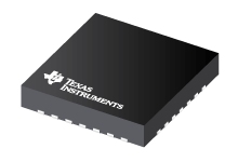
Datasheet Texas Instruments TPS65176RHDR — Ficha de datos
| Fabricante | Texas Instruments |
| Serie | TPS65176 |
| Numero de parte | TPS65176RHDR |

LCD Bias IC para TV 28-VQFN -40 a 85
Hojas de datos
LCD Bias Integrated Circuit for TV datasheet
PDF, 699 Kb, Archivo publicado: oct 16, 2012
Extracto del documento
Precios
Estado
| Estado del ciclo de vida | Activo (Recomendado para nuevos diseños) |
| Disponibilidad de muestra del fabricante | No |
Embalaje
| Pin | 28 |
| Package Type | RHD |
| Industry STD Term | VQFN |
| JEDEC Code | S-PQFP-N |
| Package QTY | 3000 |
| Carrier | LARGE T&R |
| Width (mm) | 5 |
| Length (mm) | 5 |
| Thickness (mm) | 0.9 |
| Pitch (mm) | 0.5 |
| Max Height (mm) | 1 |
| Mechanical Data | Descargar |
Paramétricos
| DisplayType | LCD Unipolar |
| IC Integration | LCD Bias |
| Pin/Package | 28VQFN |
| Source Driver Voltage(Max) | 18.5 V |
| Source Driver Voltage(Min) | 13.7 V |
| Special Function | Reset Generator |
| Target Application | 13 to 21 inches,21 inches and above |
| Topology | Boost,Buck |
| Vin(Max) | 14 V |
| Vin(Min) | 9.5 V |
Plan ecológico
| RoHS | Obediente |
Notas de aplicación
- Generation of a VCOM buffer input using PWM signalPDF, 439 Kb, Archivo publicado: dic 21, 2015
In an LCD the backlight shines through the liquid crystal material and the voltage across the liquid crystal controls how much light shines through it. An active matrix LCD (AMLCD) contains many pixels arranged in a grid pattern. The voltage across each pixel is controlled individually so that high resolution images can be created. One terminal of every pixel is connected to a common plane. The v - Understanding Undervoltage Lockout in Power Devices (Rev. A)PDF, 90 Kb, Revisión: A, Archivo publicado: sept 19, 2018
Many integrated circuits include an undervoltage lockout (UVLO) function to disable the device at low supply voltages. Below the minimum supply voltage the function and performance of a device may be undefined making it impossible to predict system behavior. This application note explains how to correctly understand the undervoltage lockout specification in the data sheets of TI's power products. - Minimizing Ringing at the Switch Node of a Boost ConverterPDF, 201 Kb, Archivo publicado: sept 15, 2006
The application report explains how to use proper board layout and/or a snubber to reduce high-frequency ringing at the switch node of a boost converter. - Basic Calculation of a Boost Converter's Power Stage (Rev. C)PDF, 186 Kb, Revisión: C, Archivo publicado: enero 8, 2014
This application note gives the equations to calculate the power stage of a boost converter built with an IC with integrated switch and operating in continuous conduction mode. It is not intended to give details on the functionality of a boost converter (see Reference 1) or how to compensate a converter. See the references at the end of this document if more detail is needed.
Linea modelo
Serie: TPS65176 (2)
- TPS65176RHDR TPS65176RHDT
Clasificación del fabricante
- Semiconductors > Power Management > LCD/OLED Display Bias Solutions