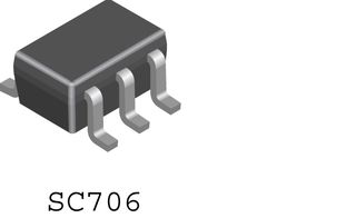
Datasheet FDG6321C - Fairchild — Ficha de datos

Part Number: FDG6321C
Descripción detallada
Manufacturer: Fairchild
Docket:
November 1998
FDG6321C Dual N & P Channel Digital FET
General Description
These dual N & P-Channel logic level enhancement mode field effect transistors are produced using Fairchild's proprietary, high cell density, DMOS technology.
This very high density process is especially tailored to minimize on-state resistance. This device has been designed especially for low voltage applications as a replacement for bipolar digital transistors and small signal MOSFETS. Since bias resistors are not required, this dual digital FET can replace several different digital transistors, with different bias resistor values.
Features
Specifications:
- Continuous Drain Current Id: 500 mA
- Current Id Max: 500 mA
- Drain Source Voltage Vds: 25 V
- MOSFET TRANSISTOR ROHS COMPLIANT: NO
- Mounting Type: SMD
- Number of Pins: 6
- On Resistance Rds(on): 450 MOhm
- Operating Temperature Range: -55°C to +150°C
- Package / Case: SC-70
- Power Dissipation: 300 mW
- Rds(on) Test Voltage Vgs: 4.5 V
- SVHC: No SVHC (19-Dec-2011)
- Threshold Voltage Vgs Typ: 800 mV
- Transistor Case Style: SC-70
- Transistor Polarity: N and P Channel
- Voltage Vds Typ: 25 V
- Voltage Vgs Max: 800 mV
- Voltage Vgs Rds on Measurement: 4.5 V
RoHS: Yes